Power electronics is a mature technological discipline, as it has been used in many industrial, transport, distribution, aerospace, commercial and domestic applications, among others, for several decades.
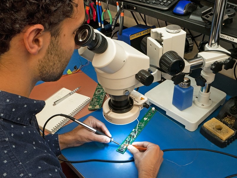
But this does not mean that new advances, new materials, new optimized designs, which lead to more reliable, faster, more robust, more efficient, more economical devices, are no longer being sought… For this it is vital to have quick and early access to reliable prototypes, as well as to the competitive manufacture of such devices.
Between 80% and 90% of the key differentiating competitive features of, for example, leading industrial and mobility suppliers depend on integrated power electronics and software.
Most prominent R&D projects in power electronics main objectives are:
- Optimize the doping elements of gallium nitride (GaN), in order to create a powerful semiconductor base that boosts the efficiency of electronic circuits, which promises to boost the manufacture of more powerful and efficient components such as LEDs and other modules used in industries such as energy, where they are used to build and manage electrical distribution networks, the same in consumer electronics.
- Expand the limits of silicon-based power technologies in 300 mm wafer diameters to optimize current limitations in the connection resistance of Trench-Power-MOSFET and IGBT devices and expand the capabilities of the 300 mm pilot lines already installed.
- Boost the technology of gallium nitride power devices thanks to their superior performance, seeking the absolute limit of GaN compared to current approaches adopted.
- Configure the pilot production line for fully processed GaN in carrier power semiconductors in a 200 mm wafer diameter that coexists and is compatible with CMOS power manufacturing capabilities.
- Develop new integration schemes that support high levels of integration and designed substrates that enable the manufacture of intelligent systems and greater integration and compact Smart-Power applications; configuration of pilot production lines for integration (packaging) of advanced gallium nitride based power product chips.
A good part of the work activities of this “Powerbase” project are fundamentally research work focused on silicon wafers, gallium nitrate doping technology, etc. However, there are others focused more on the development of applications that can be marketed with the new devices developed, manufactured in the various activities of the pilot line.

Through the use of the new devices, the intelligent systems will achieve greater efficiencies, higher switching frequencies and higher power densities. Some highly beneficial direct applications would be: LED lighting, solar inverter, energy conversion for telecommunications, battery charger and compact power supplies for automation systems…
But where does the importance of this project lie? It is fundamentally based on the fact that the estimated growth of the global market for gallium nitride (GaN) technology will generate ordinary revenues of $2.6 billion per year by 2022, becoming a segment in which the supply chain will pay special attention because it is extremely fruitful.
The technology of Gallium Nitride on Silicon deposited in highly doped substrates created at the end of the last century, facilitated the manufacture of light-emitting diodes (LEDs) of high luminosity and brightness. Many other technologies allowed the design of organic LEDs that led to the introduction of blue, purple, violet, white and UV diodes; likewise Gallium Nitride will make possible an infinity of innovation in the technology industry.
As some experts predict, the next great technology that will revolutionize power electronics after the foreseeable GaN boom will be semiconductor nanoparticles, also called Quantum Dots (QD), which are supposed to enable more effective and powerful communication with higher frequencies.
This QD technology is in a research phase, involving a good part of the scientific community, since it is considered as one of the tools that will contribute to the deployment of the so-called Fourth Industrial Revolution, characterized by novel robotic systems and more sophisticated communications.
But these particles need to work on substrates with more appropriate dielectric properties, even at an early stage of research. And gallium nitride (GaN) is, however, a technology of present development, and in full phase of competitive development, for the manufacture of semiconductor devices with possibilities of integration of future communication systems.
Several countries that are already working on aligning their industries to actively receive the production of GaN systems:
- Japan, with key companies such as Renesas Electronics, ROHM, Nichia, Chemical Corporation, Mitsubishi, Toshiba, NTT Advanced Technology, and Toyoda, which have lines of research and development for the manufacture and production of GaN semiconductors.
- In Europe: Philips, Aixtron SE and AZZURO Semiconductors AG. They are currently the most prominent companies.
- In America: Texas Instruments, Cree Incorporated, RF Micro Devices Incorporated and NXP Semiconductor; Germany.
- In short, gallium nitride (GaN) will be an important spur for the entire power electronics industry, achieving higher power densities, increasing switching frequencies, and also greater energy efficiencies.